Can ECAM Metal 3D Printing Transform Data Center Cooling
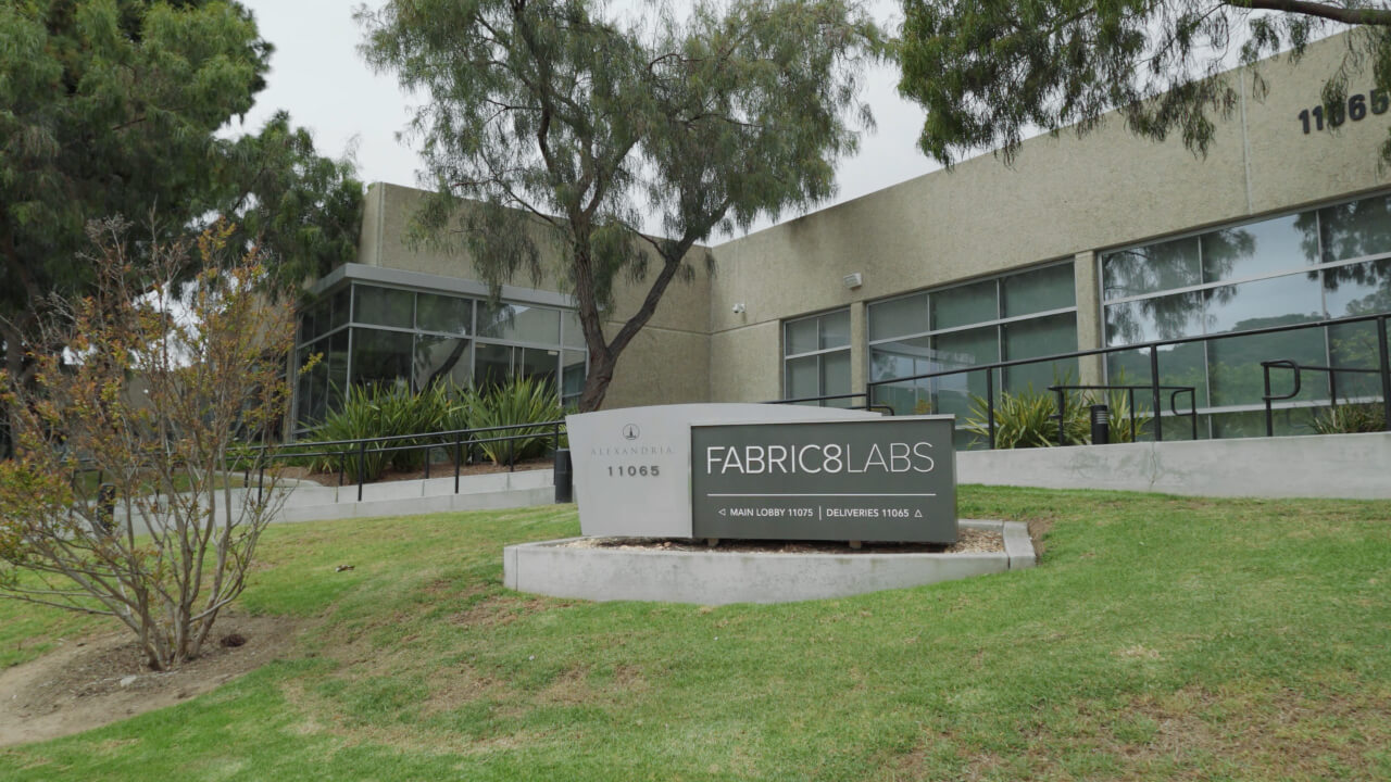
TDK Corporation announced on June 10, 2026 that it has signed a definitive agreement to acquire Fabric8Labs, Inc., based in San Diego, California, for up to 400 million USD (approximately 62.4 billion yen) in cash. The deal consists of an upfront payment and a multi-year earnout. Upon closing, Fabric8Labs will become a wholly owned subsidiary of TDK. The transaction is subject to customary closing conditions, including regulatory approvals. GTK Partners (San Francisco) served as financial advisor to TDK, and Baker McKenzie as legal counsel.
What Kind of Company Is TDK
TDK is a global electronics manufacturer headquartered in Tokyo with a history spanning more than 90 years. The company’s revenue for fiscal year 2026 reached 16.6 billion USD (approximately 2.6726 trillion yen), with approximately 107,000 employees worldwide. TDK’s product portfolio spans passive components, sensors, power supplies, lithium-ion and all-solid-state batteries, magnetic heads, and AI and enterprise software solutions.
In the data center space, TDK already supplies components such as thermal management materials, EMI suppression products, and power conversion modules. The company has positioned this area as a strategic priority amid growing data processing demand driven by AI, and its current Medium-term Plan explicitly calls for accelerating its data center business.
What Kind of Company Is Fabric8Labs
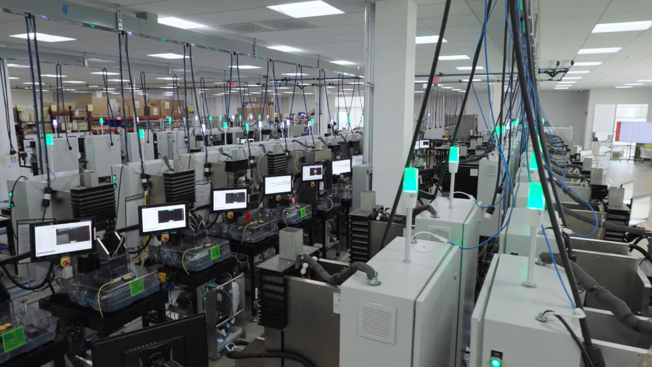
Fabric8Labs, Inc. was founded in 2015 and is led by CEO and co-founder Jeff Herman and CTO and co-founder David Pain. The company employs approximately 150 people and is headquartered in San Diego, California.
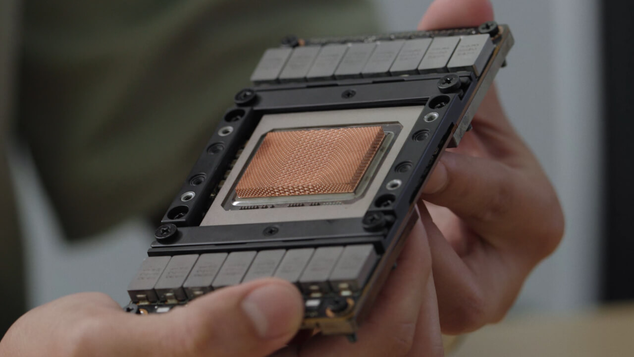
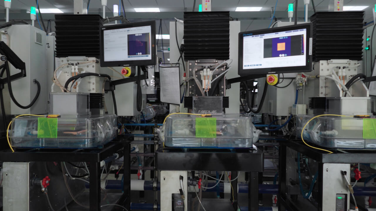
Fabric8Labs’ core technology is Electrochemical Additive Manufacturing (ECAM), a metal 3D printing process used to produce high-precision metal structures for electronics, medical devices, telecommunications, and semiconductors. In the data center space, the technology has been applied to advanced liquid cooling solutions, power management components, and semiconductor packaging.
Fabric8Labs had just closed a 50 million USD (approximately 8 billion yen) funding round on November 13, 2025, aimed at expanding US manufacturing capacity. The round was led by NEA (New Enterprise Associates) and Intel Capital, with participation from Lam Capital (the corporate venture arm of Lam Research), TDK Ventures, and SE Ventures (Schneider Electric’s venture capital fund). The funds were earmarked for scaling annual production capacity from 5 million to 22 million units. In other words, Fabric8Labs was acquired by TDK right as it entered the phase of transitioning from technology validation to mass production.
TDK’s venture capital arm, TDK Ventures, Inc., had been investing in Fabric8Labs not only in this November 2025 round but continuously since the company’s seed stage. This acquisition was not a sudden decision, but the culmination of a multi-year relationship.
Why Now
The backdrop to this acquisition is a structural shift in data centers driven by the rapid spread of AI.
Data center construction is proceeding at a record pace worldwide as generative AI adoption accelerates. According to the International Energy Agency (IEA), global investment in data centers has nearly doubled since 2022, reaching roughly 500 billion USD (approximately 80.5 trillion yen) in 2024. This construction boom runs first into the problem of electricity. The IEA projects that global data center electricity consumption will more than double by 2030, to approximately 945 terawatt-hours annually, a figure that slightly exceeds Japan’s entire current electricity consumption.
However, an even more serious problem than power supply is emerging: heat dissipation. Consuming more electricity means generating more heat. While the power problem can, to some extent, be addressed through grid expansion and investment in generation capacity, removing the resulting heat is a problem of physical design inside the data center itself, and it cannot be solved as easily. The view that conventional air cooling has already reached its limits is spreading across the industry, and this is driving a broader shift in how data centers are cooled. Market estimates vary, but the AI-related data center liquid cooling market is estimated at roughly 3.7 to 4.0 billion USD (approximately 595.7 to 644.0 billion yen) in 2026, with some forecasts projecting growth to 17.0 to 18.0 billion USD (approximately 2.737 to 2.898 trillion yen) by the mid-2030s.
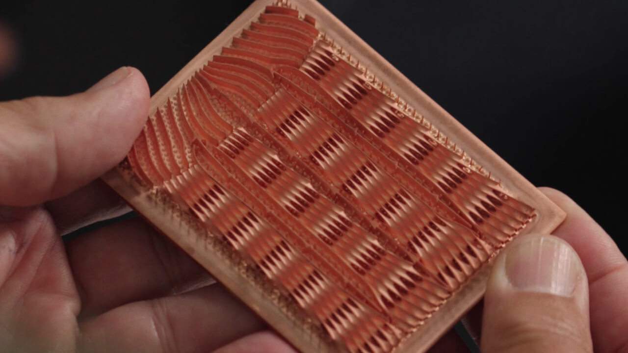
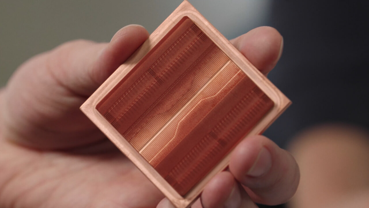
There are several approaches to data center cooling. These include rear-door heat exchangers that cool exhaust air at the back of server racks, and immersion cooling, in which server components are submerged in dedicated cooling fluid. Among these, the most widely adopted approach today is “direct-to-chip” cooling, which attaches cold plates directly to CPUs and GPUs to cool the chips with liquid. Because modern chips concentrate enormous amounts of power, they tend to develop localized “hot spots.” Cooling these effectively requires microscopic 3D fluid channels inside the cold plate. Channel sizes of roughly 30 to 150 micrometers are already used in practical, functioning systems today.
So why did TDK need Fabric8Labs’ ECAM technology on top of an approach that is already in practical use? According to TDK’s sources, ECAM-based liquid cooling solutions can reduce accelerator temperatures by up to 7°C per kilowatt compared to competing solutions, translating directly into higher silicon power density, increased rack density, improved energy efficiency, and extended component lifespan for hyperscalers and OEMs. TDK sees ECAM’s value in pushing existing cold plate technology a step further.
What Makes ECAM Different
It is worth clarifying upfront that ECAM is not simply “a 3D printing technology positioned against machining.”
In cold plate manufacturing, there is a hybrid approach in which the entire part is not built by AM (additive manufacturing) alone. Instead, a base plate is produced through machining, and only the high-value parts, such as complex internal channels and fine structures, are added using AM. ECAM itself is often used this way: adding high-resolution cooling features onto a pre-machined copper base plate, a design philosophy that limits the costly 3D printing process to only the complex sections in order to improve scalability.
There are also hybrid machine tools already in commercial use that alternate between metal laser sintering and high-speed milling within a single machine. In this approach, the milling tool finishes the internal geometry every few printed layers, achieving a machined-equivalent surface finish and accuracy combined with complex internal structures that machining alone cannot produce.
However, this approach has a limitation. Laser-based metal additive manufacturing is constrained by the size of the metal powder particles and the size of the laser’s melt pool, which together determine the smallest feature size achievable. Typical laser-based processes have a minimum feature size of roughly 20 to 50 micrometers, and even when finished with milling, this cannot exceed the resolution limit of the underlying additive process itself. For the complex heat exchange structures required in data centers, this resolution becomes a bottleneck.
ECAM takes a different approach here. Because the electrochemical deposition (electroplating) process reduces and deposits metal ions directly at the cathode surface, it is not constrained by the resolution limitations specific to laser-based methods, such as metal powder particle size or melt pool size.
Here is how it works concretely. ECAM uses an electrolyte solution containing metal ions. To build copper structures, for example, a “metal salt” such as copper sulfate, a compound containing copper ions, is dissolved in water to form the electrolyte. When electric current is applied to this solution, copper ions in the solution gain electrons at the surface of the cathode (the location being built) and are reduced into solid copper. By controlling the position of this reaction and repeating it layer by layer, a three-dimensional structure is built up.
This mechanism is easiest to understand by comparison to resin-based stereolithography (DLP-style 3D printing). In stereolithography, a projector displays one layer’s pattern at a time, curing only the resin exposed to light, building up the object layer by layer. ECAM follows the same logic, using an electrode array divided into individually controllable pixels, with each layer’s pattern controlled by which pixels carry current. In place of light, it uses electric current. In place of resin, it uses metal ions. Metal is deposited and built up only at the pixels that carry current, making it, in effect, a “metal version of DLP stereolithography.”
What fundamentally distinguishes this approach from machining or laser-based methods is that metal is neither “cut away” nor “melted and solidified,” but instead “chemically generated as a solid” from ions in solution. Because electrodeposition proceeds near room temperature, it does not produce thermal stress or distortion, and it can control geometry down to a resolution under a few micrometers, an order of magnitude finer than laser-based methods.
There is also a difference in feedstock. Laser-based metal 3D printing melts and solidifies highly refined solid metal powder using a laser. ECAM, by contrast, uses an electrolyte made by dissolving metal salts in water, rather than metal powder, as its feedstock. Fabric8Labs explains that while refining metal powder requires a dedicated process that adds cost, metal salts are commodity chemicals with an established supply chain and can be sourced more cheaply. This is Fabric8Labs’ own explanation, however, and no third-party data comparing total manufacturing cost, including equipment investment and production efficiency beyond feedstock alone, has been confirmed.
In short, ECAM’s advantage lies not in whether it can access complex internal geometries, but in how fine a structure it can resolve, surpassing the resolution limits of both machining and laser-based methods. The ability to produce micron-scale, finely optimized channel structures tailored to a chip’s uneven heat distribution, at a cost that supports mass production, is the technical core of ECAM and one reason TDK took notice.
Why an Acquisition
TDK President and CEO Noboru Saito has described Fabric8Labs’ ECAM technology as a foundational manufacturing innovation that can not only improve TDK’s existing solutions but also enable product and performance levels that were previously unattainable. He has explained that bringing this technology into TDK’s global manufacturing network, in order to deliver products that will define next-generation data center performance, represents a major advantage for customers.
This comment makes clear that TDK’s objective is not simply to procure cold plates from Fabric8Labs. It is to integrate ECAM technology itself into TDK’s manufacturing infrastructure, so that TDK’s quality systems and mass-production capabilities can be applied to it directly. Outsourcing or a technology partnership could not achieve this integration. Only full ownership allows ECAM technology to become part of TDK’s own design and manufacturing process.
AM Insight Asia Perspective
What matters in reading this acquisition is the timing Fabric8Labs found itself in. A company that had just raised 50 million USD (approximately 8 billion yen) in November 2025 and was beginning its transition to mass production was fully acquired less than a year later. This suggests there was a barrier the startup could not clear alone on the path from technology validation to manufacturing at scale.
Cooling components for data centers require quality assurance and supply reliability comparable to automotive parts, since a defect such as a leak can bring down an entire system. Hyperscalers and OEMs tend to be cautious about entering multi-year, large-scale supply agreements directly with capital-constrained startups. For Fabric8Labs, coming under TDK, with its global quality systems and manufacturing footprint, may have represented the fastest path to delivering its technology to customers at production scale.
The choice of a full acquisition, rather than a partnership, carries its own significance. Fabric8Labs had attracted investment from strategic players across the semiconductor and infrastructure industries beyond TDK Ventures, including Intel Capital, Lam Capital, and SE Ventures (Schneider Electric’s venture arm). Had TDK settled for a partnership or contract manufacturing arrangement, one of these other strategic investors could conceivably have moved first to acquire the company outright. By proceeding to full ownership, TDK closed off that path for any other investor that might have sought to capture the technology. This is a pattern visible in hindsight, and whether TDK intended it from the outset cannot be confirmed from public information. Still, given that multiple strategic investors had a stake in the technology, the risk of delaying the acquisition was likely not insignificant.
This acquisition also fits within a broader industry pattern. Johnson Controls’ announced acquisition of liquid cooling component maker Alloy Enterprises is another example of major players moving to bring advanced manufacturing technology in-house. TDK’s move belongs to this same trend: rather than remaining a component supplier, it is absorbing the manufacturing technology itself in an effort to secure a leading position in the growing data center market.